Electronic correlations and spin-orbit coupling in 2D layers and at interfaces
Project A01 within DFG Collaborative Research Center 1238
When thinned down to the 2D limit, many materials show interactions and phases quite unlike those present in their 3D realizations. The weak 2D screening leads to an enhancement of correlation effects in the layer, while a lack of inversion symmetry can lead to a spin-valley coupling and allow one to use the valley index as a carrier of information (i.e. valleytronics). Understanding and ultimately controlling the ground states of 2D materials is a research area of wide interest due to the exotic physical phenomena involved, as well as providing tantalizing prospects for future applications in optoelectronics and catalysis, for example.
We have previously developed new growth techniques for 2D transition metal dichalcogenides (TMDCs). Thereby, we are able to synthesize nearly defect-free TMDC layers on an inert graphene substrate [more]. The resulting quasi-freestanding layers exhibit close to pristine properties: MoS2 monolayers grown on graphene were measured with scanning tunnelling spectroscopy to have the largest band gap to date for supported MoS2 [more] and a very narrow photoluminescence peak compared to other growth methods [more].
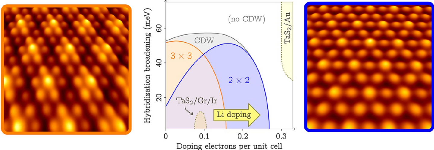
Presently, control of the electronic and magnetic phases in TMDCs is in the focus of this project. For example, we demonstrated that the nature of a charge density wave (CDW) in a monolayer of a TMDC can be controlled by the environment. A change in the CDW periodicity through Li-doping together with a full CDW phase diagram is visualized in Fig. 1 [more]. Current research is directed along three main avenues. (I) Chemical moiré engineering in order to create flat bands. (II) (Field-effect) gating so as to control the Fermi-level within the 2D system. (III) Introduction of magnetic adsorbates and layers to TMDCs with strong spin-orbit coupling to induce substantial valley-splitting.
Left: perspective view atomic resolution STM of the 3×3 charge density wave (CDW) of monolayer 2H-TaS2 on graphene measured at 5 K. Middle: CDW phase diagram calculated as a function of doping level and hybridization. Location (doping level and degree of hybridization) for TaS2 on Gr/Ir(111) is indicated. Right: perspective view atomic resolution STM topograph after additional Li doping, giving rise to a transformation of the 3×3 to a 2×2 CDW.